On April 23, 2025, Taiwan Semiconductor Manufacturing Co. (TSMC) introduced its latest AI readiness in manufacturing and packaging technologies.
A14 Process Technology
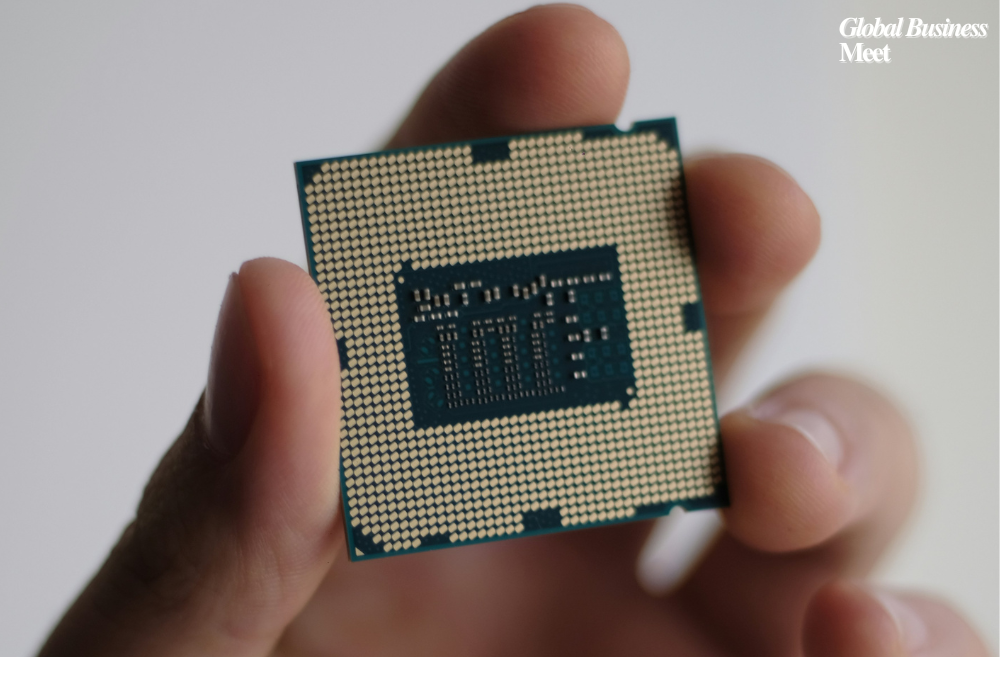
The upcoming A14 manufacturing process, designed to graduate in 2028 was announced by TSMC. Expecting to be in mass production this year, the N2 chips will deliver 15 per cent faster processing or 30 per cent less power consumption than the forthcoming tech. The A14 is the first energy efficient, high performance computing process.
System on Wafer-X (SoW-X)
TSMC also announced its “System on Wafer-X” (SoW-X) technology in addition to the A14 process. It offers to integrate at least 16 large computing chips including memory and optical interconnections into one large scale package. The SoW-X aims at offering thousands of watts of power to support the very ambitious computational requirements of the most advanced AI applications.
The newest products are further ahead of what Nvidia offers with its two chip GPUs and its soon to be released “Rubin Ultra” GPUs which bundle four chips. TSMC’s SoW-X technology gives the company an excellent position for high performance chip packaging solution by enabling much more chip integration.
Expansion in Arizona
TSMC is building those factories in Arizona to support these kind of technological progress. The expansion is a component of his wide ranging plan to launch six chip factories two packaging plants and an R D center at the site. It shows TSMC’s intention to advance its manufacturing capabilities and assist growing demand for advanced semiconductor solutions in the United States.
In this day and age of highly competitive semiconductor industry with Intel in particular racing to catch up with TSMC in the chip manufacturing the moves show TSMC’s strategic goal on innovation and in capacity expansion to stay on top.